design files prepared for PCB fabrication and assembly
Preparing design files for PCB fabrication and assembly is a crucial step in the development of a printed circuit board. These files serve as the blueprint for the entire manufacturing and assembly process, guiding everything from the creation of the PCB itself to the accurate placement of components during assembly. The preparation of these design files involves several steps, each of which ensures that the final PCB will meet the required specifications and perform as expected.
The first stage in preparing design files for pcb fabrication and assembly begins with the creation of a schematic diagram. This diagram illustrates the electrical connections between all the components on the PCB, including resistors, capacitors, ICs, and connectors. The schematic serves as the foundation for the design, outlining how the electrical signals will flow across the board. Designers use specialized PCB design software to create this schematic, ensuring that all components are correctly linked and that the circuit functions as intended. The schematic is then used to generate a netlist, which is a detailed list of all the electrical connections in the design.
Once the schematic is complete, the next step is to create the PCB layout. This layout defines the physical placement of components on the PCB, as well as the routing of the electrical traces that connect them. The layout must take into account several factors, such as the board’s size, component size and orientation, trace width, and spacing between pads. Designers must also consider factors like signal integrity, thermal management, and power distribution when designing the layout. Advanced PCB design software is used to create and optimize the layout, ensuring that all the necessary components fit within the design constraints and that there are no issues with signal interference or heat dissipation.
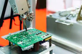
How are design files prepared for PCB fabrication and assembly?
After the PCB layout is designed, the next step is to generate the necessary design files for fabrication. These files, often in the Gerber format, provide all the information needed for the PCB manufacturer to fabricate the board. The Gerber files contain details about the copper layers, drill holes, solder mask, silkscreen layers, and other essential features of the PCB. These files are created by the PCB design software and are reviewed for accuracy and completeness before being sent to the manufacturer. It is crucial that these files are generated correctly to avoid errors during fabrication, as even small mistakes in the design files can lead to defects in the final product.
In addition to the Gerber files, manufacturers also require an assembly drawing or bill of materials (BOM) to guide the placement of components during the assembly process. The BOM lists all the components used in the PCB design, along with their specifications, such as part numbers, values, and package types. The assembly drawing provides detailed information on where each component should be placed on the PCB, including component orientation and alignment. This ensures that the pick-and-place machines used during assembly can accurately position components on the board.
Once the design files are prepared, they undergo a thorough verification process. This process, often referred to as Design Rule Checking (DRC) and Electrical Rule Checking (ERC), ensures that the design meets the necessary manufacturing and performance requirements. DRC checks for issues like trace width violations, spacing violations, and unconnected pads, while ERC ensures that the electrical connections are correct and functional. These checks are crucial for preventing errors that could lead to manufacturing defects or functional problems in the final PCB.
After the design files have been verified and approved, they are sent to the PCB fabrication and assembly team. The manufacturer uses these files to create the physical PCB, following the layout and fabrication instructions. For assembly, the files guide the precise placement of components, ensuring that the board is populated accurately. The process of preparing these design files is essential for the successful production of a high-quality PCB that meets the required specifications for both functionality and reliability.