thermal management in electronics circuit boards
During the course of passing from one layer to another in a printed circuit board (PCB), electricity generates heat. The amount of heat it creates depends on how much resistance it encounters on its way through the circuit. High currents, traces and power components usually produce more heat than their lower-power counterparts. These hotspots need to be cooled in order for the PCB to function properly. Insufficient cooling can lead to a variety of problems, including a change in impedance and even signal distortion. To prevent overheating, designers use a range of techniques to manage the flow of heat through the circuit board. These include thermal pads, thermal vias and cooling fans. These technologies are commonly used in high-power, high-speed devices.
PCB designers use thermal analysis tools to determine if additional cooling methods like fans, heat sinks or thicker layers of copper are necessary to keep the temperature of active components within acceptable limits. The goal is to achieve a good balance between performance and reliability by choosing the best materials, manufacturing processes and PCB layout for the given application.
The use of advanced electronics circuit boards components and the ongoing trend towards miniaturization are two of the main factors that increase the need for better thermal management solutions in electronics. Modern electronic devices feature power-hungry processors, high-power LEDs and HD screens, 5G and WIFI transmission systems and many other advanced functions that require a lot of energy to operate. These elements all produce a significant amount of heat, which can be problematic for the overall device reliability.
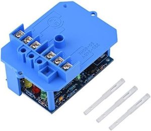
How do you handle thermal management in electronics circuit boards?
In addition to affecting the operation of the component, excessive heat can also cause solder joints to expand and contract at different rates, which can damage their physical integrity. Insufficient cooling can also affect the stability of conductive metals, especially those with very high current flows.
Depending on the type of electronics, certain cooling methods are more effective than others. For example, thermal vias are padded holes in the PCB that can be filled with a conductive epoxy and plated over, making them great for quickly channeling heat away from power dissipating components. They can be arranged in a grid to maximize their thermal dissipating potential. Moreover, alternative substrate materials with a higher thermal conductivity can be used to decrease the junction temperature and component temperatures.
A thermal camera is a useful tool for inspecting the condition of a PCB after assembly. It enables you to identify hotspots on the surface of the PCB, and it can also be used for thermal simulation during the design process. Thermal cameras can also detect areas of the board with high electrical stress, which is a sign that a solder joint is in poor condition and could fail under prolonged mechanical stress.
The most important aspect of managing the flow of heat in a circuit board is the correct choice of materials and design placement. Properly designing a stackup, defining ground planes and copper pours, using appropriate package sizes, and placing components with proper mounting pads are the most effective thermal management methods for reducing the heat generated by active components on a circuit board.