multi-layer PCB in PCB fabrication assembly
A multi-layer PCB (Printed Circuit Board) is a type of circuit board that contains more than two layers of conductive material, typically copper, separated by insulating layers, often made of epoxy resin or other materials. These boards are designed to support complex circuits and components while optimizing space, reducing interference, and enhancing performance. Multi-layer PCBs are commonly used in applications that require high-density circuits, such as computers, smartphones, automotive systems, medical devices, and telecommunications equipment. In the PCB fabrication assembly process, the production and assembly of multi-layer PCBs require precise design, advanced manufacturing techniques, and careful handling to ensure that the final product meets performance and reliability standards.
The primary advantage of a multi-layer PCB in PCB fabrication assembly is its ability to accommodate a large number of electronic components in a compact space. With traditional single-layer or double-layer PCBs, the design is often limited by the available space on the board. However, multi-layer PCBs allow for additional layers to be incorporated, each of which can carry its own circuit traces, providing more space for routing connections and components. This is especially beneficial for modern electronic devices, which require compact, high-performance circuit boards with minimal size. As a result, multi-layer PCBs enable more complex and powerful devices to be produced, while still maintaining efficient use of space.
In the PCB fabrication assembly process, the creation of a multi-layer PCB involves several key steps. The first step is designing the circuit board layout, which includes determining how many layers are needed based on the complexity of the circuit. Multi-layer PCBs typically have anywhere from three to twelve layers, depending on the design requirements. Once the design is finalized, the PCB fabrication assembly process begins with the preparation of the individual layers, which are usually produced as separate single-layer PCBs. These layers are then stacked together, and precise alignment is crucial for ensuring that all layers are properly connected. After stacking, the layers are bonded together using high-temperature presses, with an insulating material between them to separate each layer.
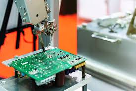
What is a multi-layer PCB in PCB fabrication assembly?
The process of via drilling is also a critical step in multi-layer pcb fabrication assembly. Vias are small holes drilled through the PCB to connect the different layers electrically. There are several types of vias, including through-hole vias, blind vias, and buried vias, depending on how the layers are connected. Through-hole vias go all the way through the board, while blind and buried vias are used when connections are needed between specific layers. The proper placement and drilling of vias are crucial for ensuring that the circuit works correctly and that there are no shorts or open circuits.
One of the significant challenges in multi-layer PCB fabrication assembly is ensuring the electrical and mechanical integrity of the board. The alignment of the layers, proper via placement, and ensuring good electrical connections between layers are essential for the board’s performance. To achieve this, specialized equipment and precise manufacturing processes are used, including automated optical inspection (AOI) and X-ray inspection systems. These systems help identify any defects, such as misaligned layers or poorly soldered connections, which can lead to functional issues in the final product.
Multi-layer PCBs also offer the benefit of improved signal integrity. With modern electronic devices becoming increasingly complex, it is essential to minimize interference between components and circuits. Multi-layer PCBs can incorporate dedicated power and ground planes within the design, which helps to reduce noise and improve signal quality. By using multiple layers, designers can isolate sensitive signals, reducing the likelihood of signal degradation and crosstalk between traces. This is particularly important for high-frequency applications, such as communication devices or high-speed computing systems, where maintaining clean signals is crucial.
Another advantage of multi-layer PCBs in PCB fabrication assembly is their ability to enhance thermal management. As electronic components generate heat, it becomes increasingly important to design PCBs that can effectively dissipate this heat. Multi-layer PCBs can incorporate thermal vias and copper planes that help to distribute heat more evenly across the board, preventing overheating and improving the reliability of the components. This feature is particularly beneficial for power-hungry devices that generate significant amounts of heat, such as processors, graphics cards, and power supplies.
In conclusion, multi-layer PCBs play a vital role in the PCB fabrication assembly process, offering significant advantages in terms of space efficiency, signal integrity, thermal management, and overall performance. Their ability to accommodate complex circuits in a compact design makes them essential for modern electronic devices. However, the fabrication and assembly of multi-layer PCBs require advanced techniques, precise manufacturing, and careful attention to detail to ensure that the final product meets the required performance and reliability standards. As electronic technology continues to evolve, multi-layer PCBs will remain a critical component in the development of high-performance, miniaturized devices.